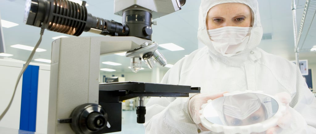
Visual Microscope Inspection in Semiconductors: The Challenge Has Changed
An insight into why visual microscope inspection remains critical in semiconductor manufacturing, exploring the challenges of shrinking geometries, decision consistency, and the growing role of intelligent inspection tools in protecting yield and quality.
Jamie Greatrix | Founder & Director of JAIMS
12/17/20253 min read
Visual Microscope Inspection in Semiconductors: The Challenge Has Changed
Visual microscope inspection has always played a role in semiconductor manufacturing, but its importance, and complexity, has increased significantly in recent years.
As device geometries continue to shrink, structures become more three-dimensional, and production volumes increase, the challenge is no longer simply seeing defects. The real challenge is making repeatable, high-confidence inspection decisions at scale, without slowing production or introducing subjectivity into the process.
From “Can We See It?” to “Can We Decide Consistently?”
Historically, advances in semiconductor inspection were driven largely by optics: higher magnification, better illumination, improved contrast, and cleaner images. Those fundamentals are still essential, good inspection always starts with good image quality.
What has changed is the context in which inspection decisions are made.
At advanced nodes, many defects are:
Subtle and low-contrast
Borderline in terms of accept/reject criteria
Highly process-dependent
Critical to yield, even if visually minor
In this environment, the question is no longer can the microscope resolve the feature?
It is can the organisation make the same decision, every time, across operators, shifts, and sites?
The Pressure of Shrinking Geometries and 3D Structures
Modern semiconductor devices introduce inspection challenges that did not exist even a decade ago:
Extremely fine line widths
Complex 3D topographies
Advanced packaging and interconnects
Sensitive surfaces prone to contamination or damage
Visual inspection is often used to validate process steps, investigate excursions, or support yield analysis. The margin for interpretation is small, and inconsistent decisions can quickly translate into lost yield or unnecessary scrap.
This places visual inspection firmly within the process control loop, not just as a final check.
Operator Consistency Remains a Critical Risk
Even in highly automated fabs, visual inspection frequently relies on human judgement, particularly for:
Surface anomalies
Pattern defects
Edge damage
Contamination and foreign material
Two experienced operators can legitimately interpret the same image differently, especially when defects sit close to acceptance limits. Without clear standards and reliable tools, this variability becomes a risk to both quality and throughput.
This is why consistency, not just resolution, is one of the most important challenges in semiconductor visual inspection today.
The Growing Role of AI as Decision Support
AI-assisted inspection is increasingly being adopted not to replace operators, but to support consistent decision-making.
When implemented correctly, AI tools can:
Highlight regions of interest automatically
Pre-classify common defect types
Reduce inspection time
Improve repeatability across users
Localised AI training allows fabs to tailor models to specific processes and products, while cloud-based approaches support standardisation across multiple sites. In practice, many manufacturers use a hybrid approach to balance control, security, and scalability.
The key point is that AI shifts visual inspection from a purely subjective task to a data-supported decision process.
Visual Inspection as a Source of Data, Not Just Images
In modern semiconductor manufacturing, inspection results must be:
Traceable
Auditable
Linked to process steps and lots
Available for root-cause analysis
Visual inspection systems are increasingly expected to integrate with MES and quality systems, ensuring that inspection outcomes contribute meaningfully to yield analysis and continuous improvement.
A microscope that produces excellent images but cannot support traceability or standardisation is no longer sufficient in advanced fabs.
The Risk of Underestimating Visual Inspection Capability
One of the most common issues seen is the assumption that any microscope is “good enough” for visual inspection. In semiconductor environments, this is rarely true.
Sub-standard equipment, inconsistent setups, or poorly defined inspection criteria lead to:
Missed or misclassified defects
Inconsistent release decisions
Increased rework and investigation time
Reduced confidence in inspection results
Over time, this undermines both yield and trust in the quality system.
Final Thoughts
Visual microscope inspection remains a critical part of semiconductor manufacturing, but its role has evolved. It is no longer just about magnification or image clarity, it is about repeatability, decision confidence, and integration into the wider quality and process control framework.
The most successful manufacturers recognise visual inspection as a strategic capability. When supported by the right equipment, standardised workflows, and intelligent software, it becomes a powerful tool for protecting yield, quality, and business integrity in an increasingly demanding industry.
Contact
Questions? Reach out for tailored advice.
Phone
© 2026. All rights reserved.
Company Number: 16933717
Follow us!